Computer Design Laboratory

ECE3710, CPSC 3710


General Information

  • Instructor: Priyank Kalla
  • Lectures: T, Thu, 3:40pm-5pm.
  • Venue: WEB 110 and Junior Hardware Lab (JHL) MEB 3133.
  • For the first few lectures, we will meet in the classroom WEB 110. Once we start working on the assignments, we will meet in JHL all the time. As I will show you some architecture design and Verilog coding styles, it will be easy to work hands-on in the labs. Please attend all lab sessions.
  • TA: Steven Brown
  • Labs: JHL MEB3133
  • Textbook: There are no textbooks required.
  • Pre-requisites: ECE/CS 3700, ECE/CS3810 or equivalent classes, and Verilog.

    Verilog versus VHDL

  • We are planning to use Verilog for this course. One of the main reasons is continuity following the ECE/CS 3700 course. Secondly, there is this issue of legacy, and quite a bit of Verilog support infrastructure was developed for our boards, and that will certainly come in handy. If some students have no Verilog background, but extensive VHDL background, then I **may** allow VHDL, but I must admit that if you know VHDL, you'll pick-up Verilog in a day or so and you will find it less tedious than VHDL.
  • If you know neither VHDL not Verilog, please come talk to me.

    Class mailing list

  • A class mailing list 'ece-cs-3710@lists.utah.edu' has been created to communicate with the whole class. Of course, each student will have to "subscribe" to this list to be able to send and receive messages.
  • To subscibe to this list, you should do the following:
  • You will be asked to confirm your subscription request before it can be processed. Please conform to the instructions contained in the message you receive.
  • You'll receive a welcome message, and that should be it.

  • If you just need to contact me and/or the TA, just send an email to us.

    Course Description

    Course Objective

  • As the title says it all, students will design, develop and test a Digital Computer. Students will work in groups of 3 (may have to accomodate one group of 2 or 4 students) and step-by-step design a fully functional digital computer. The design specifications will be given by me in the class, and we will review the machine organization in the lectures. It would be your job to then interpret the specifications and develop a model of the design using Verilog-HDL. The model should be simulated, and once validated, it is to be synthesized onto the FPGA boards. Finally, the implemented model should be tested for functional correctness, and subject to its proper functioning, you will all feel proud of yourselves. The design will be complete insofar as it will contain: Instruction Set Design, Memory Organization, ALU design, (Micro?)control, and Input-output design. The skills that you have learnt in ECE/CS 3700 and in ECE/CS 3810, you are going to put them to good use. We are going to implement a "simpler" model of the CR16A Microprocessor.

  • There is going to be a baseline instruction-set that every team will have to implement. Subsequently, each team may have to augment their instruction set depending upon the type of applications they have in mind.

  • In addition to the basic processor design, each student team will develop IO + memory interfaces, along with necessary drivers that will control the interfaces. Moreover, each team will propose further extensions to their designs for the applications that they particularly target. You will have enough leverage to come up with your own applications and extensions. For example, you can develop games, do some awesome graphics/visualization (SVGA interfaces), audio signal processing (interfacing audio CODECs), study and implement basic pipelining, or design fast/efficient arithmetic components. The choice is yours. Make sure that your extensions somehow relate to your applications.

    One of the main objectives of this class is to design an "application" that will run on your computer. More often than not, students have designed GAMES as the software that runs on the CPU: these have included a game of skiers trying to ski down a slope while avoiding abstacles, rock-paper-scissors, ping-pong, tank battlefield, among many other configurable and modular games. Students have also designed music synthesizers, applications to control stepper motors and such. Sometime around the last week of September or first week of October, each group of students will decide on an application.

    Then we will have a mid-semester presentation on what you have done so far (what, how, why, problems faced, workarounds, etc.) and what application you intend to design on your CPU. Once decided, then you will proceed towards writing assemblers + software for your code. Each group, and every member of the group will have to make a presentation to the class.

  • Course Deliverables: You will submit a final report at the end of the semester, make a presentation to the whole class, and demonstrate a functioning design.
  • Good news: No HWs/exams, just a whole lot of hands-on-learning :-)

    Grading

  • Your Basic CPU (ALU, Regfile, Control, Memory-access) works: 30%. (10% reports, 20% for Lab check offs).
  • Mid-Semester presentation, Project proposal & Review: 10%
  • Peripherals: 20% (PS2, Nintento keybd, SVGA, Audio CODECs etc.)
  • Software (Assembler + application programs) or dedicated hardware design: 20 %
  • Final Demo: 10% (The whole thing works together)
  • Final Report: 10%.

    Laboratory Sessions

  • Initially the students will be working with Verilog description and simulations. For this purpose, we will use the Xilinx ISE tools tools. In the JHL, version 14.7 is installed, which you can download on your own machines and use it, if you wish.

    FPGA Boards + Lab Manuals

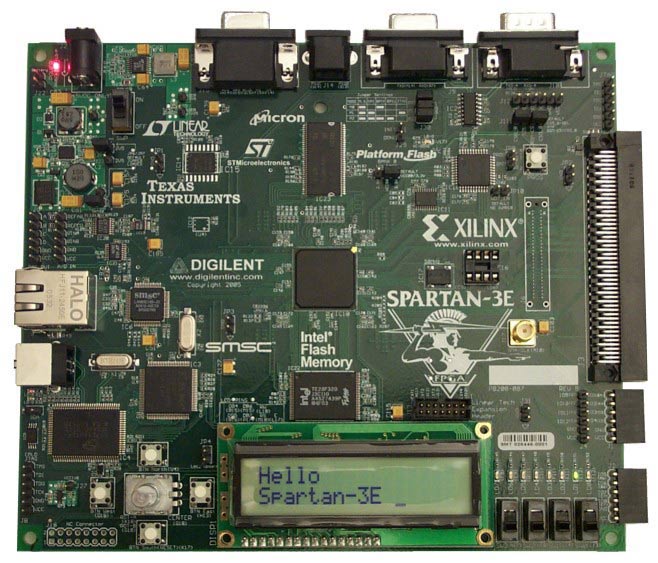
  • For this class, we have an option to use two different boards. One of the boards is the Nexys 3 board that most of you used in 3700 in S'15. The other board is a slightly older board, the Spartan-3E starter board, but it has a LCD screen interface that can help with debugging your initial development.
  • Both boards are quite powerful. You have a lot of (fast) logic available to do interesting designs, + interesting interfaces like an LCD display, PS2, RS232, Audio interfaces, Flash, Block-ram, etc. We will discuss their capabilities and uses in class.
  • By default, I would suggest you use the Nexys3 board.

    The Nexys Boards

  • Here is a link to the Nexys 3 reference manual: http://www.digilentinc.com/Data/Products/NEXYS3/Nexys3_rm.pdf .
  • Here is a link to the Nexys 3 main page: http://www.digilentinc.com/Products/Detail.cfm?NavPath=2,400,897&Prod=NEXYS3&CFID=302233&CFTOKEN=87818199
  • The Nexys 3 board uses the Spartan-6 XC6SLC16 FPGA. This document describes the architecture of this FPGA.

    The Spartan-3E starter board

    Following are a few links to the boards and associated manuals:
  • Here is the link to the Spartan 3 Starter boards .
  • On the page you will also find the users guide and also the schematic. The users guide is pretty good and contains a lot of information on how to use the peripherals.
  • Some devices share common signals and (sub-) busses on the board. A list of some of these conflicts can be found here .

  • You can access the Spartan-6 and Spartan 3E FPGA family Data-Sheets from here .

  • Also linked below is a (UPDATED) tutorial prepared by my former TA Paymon that will be very helpful: UPDATED tutorial. The last part of the tutorial on synthesis is still being prepared, but this is good to get you started with schematic capture and simulation.
  • Finally, here is a link to a large number of application notes that will be helpful in designing FIFOs, Reg-Files, using Block-RAMs etc.

    Class Handouts

  • Intro to the course.
  • PDF Version of the CR16 Programmers reference Manual . This is a generic model of a scalable RISC architecture. We are going to implement a 16-bit processor which will, in a way, resemble almost all the functionalities of the design. The programmers manual tell you all about the instruction set, types of registers and addressing modes, etc. If you have studied 3810, you'll understand almost everything in this document. In the lectures, we will look at the entire architecture and I'll give you directions on how to simplify and develop the design.
  • PDF Version of the CR16 Instruction Set Architecture .
  • Here is a simple Tutorial that one of my former TA in 2007 (Neal Tew) had created on how to download the design on the FPGA board. Its a ZIP file that you can download and extract.
  • Here is another piece of Verilog Code that Neal had developed that demonstrates how to use the on-board LCD to display characters. You can use this piece of code and modify it to suit your needs. Download Neal's LCD controller.

    Some slides describing the Spartan 3 FPGA Chip

  • Spartan3ex6.pdf

    Some slides describing Other IOs and Peripherals

  • OtherIOx6.pdf

    Course Organization and Class Schedules

  • Here is a tentative class schedule:

    8/25 - 8/27: Course intro + ISA + FPGA Board intro + Assignment I

    9/1-9/8: ALU Design + Testing

    9/10-9/22: Regfile design + ALU integration

    9/22-10/1: Memory Interface and CPU Control

    10/6-10/8: Mid Semester Presentations

    10/10-10/18: Fall Break

    10/20-11/5: Fetch + Decode + Control + Datapath integration

    11/10 - 11/24: VGA + Peripherals + software development

    11/26 onwards: Software application + final assembly

    12/10: Final Demo day!


    Laboratory Assignments

    Lab Assignment 1: ALU Design

  • [Updated Aug 27, 2015] Here is lab assignment 1, design of the ALU. Please brwose through the Programmer's reference and also the look at the ISA .
  • I will give you some basic guidelines on how to code the ALU in Verilog, and how to design the testbenches.
  • A paper that describes some issues with the use of signed arithmetic and signed typecasting in Verilog, with a few examples can be accessed here .
  • Here I am attaching my sample alu.v and alutest.v files that show how to use the $signed construct for 2'C arithmetic and the use of $random, $monitor/$display statements.

    Lab 2 Assignment - ALU + Register file Integration

  • [Updated Sept 8, 2015] Design Register file bank, and interface it with the ALU.
  • Here is lab assignment 2 ALU + Regfile integration
  • Once your ALU+Regfile combine is working, you will have to demonstrate some functioning test programs on the FPGA board. One program that you can try is testing your "RegfileRead --> ALU Op --> RegfileWrite" with a Fibonacci Sequence. My former TA, Andrew, had prepared a document describing one such setup. You can download it here . You will have to interface your datapath with an FSM - which implicitly runs your Fibonacci program - and hook-up one of the read ports to the LCD controller, if you are using the older Spartan board. Sample LCD controller can be downloaded from here . On the newer Nexys board, there is no LCD, but you could use the 7-segment LEDs to display your results, probably in hex.

    Lab Assignment 3 - Memory Interface with the CPU Datapath

  • Mapping of the BlockRAM or the Pseudo-Static (Cellular RAM) for instruction and data read and write. Interface the RAM with MAR/MDR, PC, IR, etc. to build the load/store logic.
  • In this Lab assignment, our objective to write and read data to/from memory. In the next lab, we will integrate it with the CPU.
  • We should be able to demonstrate a set of read/write operations on the FPGA board. You may use whichever memory you prefer.

  • [Updated Sept 8, 2015] Here is your Lab 3 assignment . Please get your memory working and demonstrated by Sept 29.
  • Synthesize this file memory.v and see to it (Technology Schematic) that it is mapped to a Block-RAM. This file needs to be modified for true dual port memory access, with proper write modes.
  • Here is a good description of the $readmem system tasks.

    If you want to use the Block RAM
  • Here is the description of Spartan-6 Block RAM. Please go through it.
  • Refer to the Document Libraries Guide for the Block RAM Macros
  • Attempt a configuration of 16-bit words, as given in the users guide.
    If you want to use the Cellular RAM, Paymon found the following materials
  • Here is an application note on the Cellular RAM interface
  • An entire Verilog infrastructure (zip file) for the cellular RAM interface application with video pipeline.
  • And some notes on the Cellular RAM itself.

    [Updated Tuesday Oct 20] Lab Assignment 4 - CPU Control

  • Lab 4 assignment, design issues to consider, demo and report submission instructions .
  • CPU demo on FPGA: Nov 3. Lab4 report submission on Canvas is due Friday Nov 6.

    Lab Assignment 5 --- Interfacing SVGA/PS2/Audio/Whatever to the CPU

  • Once you decide upon what applications you intend to design and implement, you will have to design interface machines/logic for external IOs. Here is a time-table that we need to strive for:
  • Paymon has prepared a good tutorial on VGA: Download it from here. Also provided is a "skeleton" Verilog code interface that you can use.
  • VGA Documentation: For our Nexys-3 board, pages 15 - 17 of our Nexys 3 documentation also describe VGA timing. For the older S3E board, refer to page 53, chapter 6 in the S3E users guide for the VGA documentation. It is a simple 3-bit RGB interface with HSynch + Vsynch pulses.
  • PS/2 Documentation is given in chapter 8, page 61 of the same document. You can assume 1-way (keyboard to CPU) communication for your designs.
  • Some more detailed info on PS/2 can be found at the following website: www.computer-engineering.org/ps2protocol .
  • RS232: While there is loads and loads of RS232 related stuff on the web, including at "wikipedia", here is a document that describes how a run-down UART can be built. The "assignment" in this document can serve your purpose as far as this lab is concerned.
  • Designing a random number generator: LFSR - will cover in class (11/15).

    [Updated Friday Dec 11] Final Project Completion, Demo and Documentation Instructions

  • Final demo, in lab, Friday 12/11, 10am-12pm. I will invite ECE and CS faculty to view your projects.
  • Final Project (archive) and the Project Report Submission Instructions and Guidelines are described in this document.
  • Download this confidential teamwork evaluation form and submit it to me along with your report.
  • Final Submission Deadline: Dec 19th, by 5pm. Submit earlier of possible.

    Verilog Related

    There are a lot of books available on Verilog. Try searching on the net and you will get confused. I'm listing a couple of books that are available in our library and, I believe, they describe Verilog from a "System Design Perspective". Some of them are dedicated to coding styles.
  • Verilog digital system design - by Zainalabedin Navabi. (Good description of event driven simulation, blocking and non-blocking assignments, and other basic concepts.
  • Verilog HDL : a guide to digital design and synthesis - Samir Palnitkar. This book is awesome. I learnt Verilog through this book.
  • Verilog styles for synthesis of digital systems - David R. Smith, Paul D. Franzon. I've not read this book, but I do know about the authors. These Professors have developed high-quality advanced Courses on Verilog Design, CAD & Synthesis.
  • A Verilog Tutorial from Bucknell University.
  • http://www.verilog.net . The name says it all. Click on the DOCS and tutorial links, and you'll find everything that you will need.
  • Another good website for loads of Verilog related stuff, including tutorials, examples, FAQs, etc. Verilog Info from ASIC world .