Biography
Kenneth S. Stevens received a B.A. degree in Biology and B.S. in
Computer Science in 1982, and M.S. in Computer Science in 1984 from the
University of Utah. He
received his Ph.D. in Computer Science from the University of Calgary, Alberta,
Canada, in 1994. From 1984 through 1991 he held research positions at
the Fairchild/Schlumberger Laboratory for AI Research, the Schlumberger
Palo Alto Research laboratory, and Hewlett Packard Laboratories in Palo
Alto CA. Dr. Stevens became an Assistant Professor at the Air Force Institute of Technology (AFIT)
in Dayton OH in 1994, and since 1996 he has been an Adjunct Professor.
Since 1996 he has been employed at Intel's Strategic CAD Labs in
Hillsboro OR.
Dr. Stevens has been on the technical program committee for various
conferences and workshop, such as the International Symposium on
Advanced Research in Asynchronous Circuits and Systems (ASYNC) where he
has served since 1998. He has been invited to be a panel member at
International Test Conference (ITC) and ASYNC. He was the principal
author and developer on three papers that received the Best Paper awards
for communication chip architecture, circuit design, and timing
analysis. He holds seven patents in the area of communications chip
design, circuit design, and timing analysis. He is a Senior Member of
IEEE. Ken has fabricated several large fully asynchronous VLSI chips,
and has developed public domain software for the international spell
checker "ispell". He is also been the co-founder of a successful small
software company. His research interests include asynchronous circuits,
VLSI, architecture and design, hardware synthesis and verification, and
timing analysis.
[home]
 |
RAPPID
Revolving Asynchronous
Pentium® Processor
Instruction Decoder
|
Project Description
The RAPPID chip is an asynchronous Pentium II instruction length decoder
and steering unit designed at Intel's Strategic CAD Lab (SCL). The
design goal was to research the feasibility of achieving
high-performance microprocessor design using asynchronous circuits. The
design was fabricated in Intel's 0.35 micron process, with silicon
arriving in June of 1998.
The RAPPID core contains 120,000 transistors in an area of 3.0 by 2.4
mm. The entire test chip circuitry (which includes instruction FIFO and
pads) contains 220,000 transistors in an area of 3.5 by 3.1 mm.
Simulation results show that RAPPID can decode instructions at an
average throughput of 3.5 instructions per nS with a latency of 2.1nS,
which is about three times better than the performance of an x86
processor running at 400MHz. (This was the frequency of the industry
leading products at the time.)
Asynchronous design has some potential benefits in areas like
performance, power, and productivity. However, the relative simplicity
of traditional clocked circuit design, in addition to lack of expertise
and tool support for asynchronous design, has thus prevented its
widespread use in microprocessors. Full adoption of asynchronous
protocols by microprocessor designers will probably not occur unless
they hit a wall that blocks further performance improvement in clocked
design. However, circuit designers are already using asynchronous
self-timed circuits to overcome the problems posed by very high
frequency clocked design. The purpose of the asynchronous design
research is to find out how to design without a clock in order to bypass
the clocked design wall. This work also focuses on developing
methodology and CAD tools to support current and future high-performance
self-timed circuit technology.
Results Summary
The following table compares the asynchronous RAPPID chip against a
400MHz processor - the fastest commercial x86 processor at the time
silicon was received. The RAPPID results - excluding testability - are
measured silicon. While the comparisons are valid, they are not
completely apple-to-apple as there are some differences between the
commercial processor interfaces and the RAPPID interfaces. However,
this is as close a comparison as has been published in academia or
industry.
| Category |
400 MHz x86 |
RAPPID |
Improvement |
| Performance (inst/nS) |
1.2 |
2.5-4.5 |
300% |
| Latency (nS) |
5.0 |
2.1 |
225% |
| Power (nJ per inst.) |
164 |
80 |
200% |
| Area (sq. mm) |
6.03 |
7.10 |
-18% |
| Testability (pseudo stuck-at) |
- |
95.9% |
n/a |
Notes:
Silicon arrived in June 1998. Unfortunately there was an undersized gate
which didn't permit the enabling of the length decode cycling from
reset. We were able to activate the part after performing a FIB edit.
The results were measured on the FIB edited silicon. A second timing bug
in the slow clocked PLA did not permit us to run the rare instructions.
Both RAPPID and an Intel processor used for comparison were fabricated
in the same line using a 0.35 micron technology.
Performance was measured at nominal Vcc and temperature, while the
clocked performance include the T-spec margins. It is not necessary to
add the margins to RAPPID because an asynchronous circuit will actually
run faster under such circumstances.
Power was measured comparing the integer power test from the P6 power test
suite. We calculated the energy per instruction in joules since the
frequencies were vastly different between the two parts.
RAPPID's area is compared to the area of the logic performing the
equivalent functionality in the clocked circuit. These parts were in
the Instruction Fetch and Decode units. There are some microarchitecture
differences and requirements, particularly in the steering logic, which
affect these results.
We designed a BIST test structure but did not fabricate it. Testability
results were calculated by feeding the BIST vectors into RAPPID using
the COSMOS fault simulator. The reported results removed intra-gate
stuck-at faults according to industry methodology. We additionally
removed from consideration faults which were not targeted by the BIST
logic (mainly prefix handling logic that accounted for approximately 4%
of the circuitry).
Schmoo results
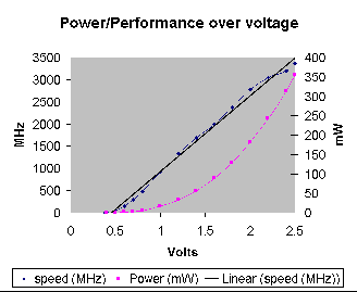
Some performance and power schmoos of the instruction delivery FIFO
circuitry on the ultra slow wafer split. The tested circuit show good
robustness over voltage. The RAPPID instruction ring FIFO performed at
1.68 GHz at 1.4V. The performance was then measured over a wide range of
voltages. The performance scaled linearly with the voltage from 2.5 volts
down to 0.5 volts, with performance ranging from 3.37 GHz down to 47 MHz.
Under 0.5V - 0.6V, the performance no longer scaled linearly and the part
became unreliable.
Power was measured across the operating range for a single low activity
data point. The power ranged from 354mW at 2.5V to 55.6mW at 1.4V,
16.2mW at 1.0V and 0.22mW at 0.5V. These power numbers in particular are
preliminary because of the sensitivity to data dependencies and activity
factors. These numbers show scaling and a single datapoint but are not
complete and run on a low activity test.
Following are graphs of measured silicon performance and power
results:
Performance of the ultra-slow wafers seem to be very close to the slow
split simulations we ran.
Comments are welcome. Please send e-mail to
kstevens@ece.utah.edu
Copyright © 2000 - All rights reserved
Last Modified: